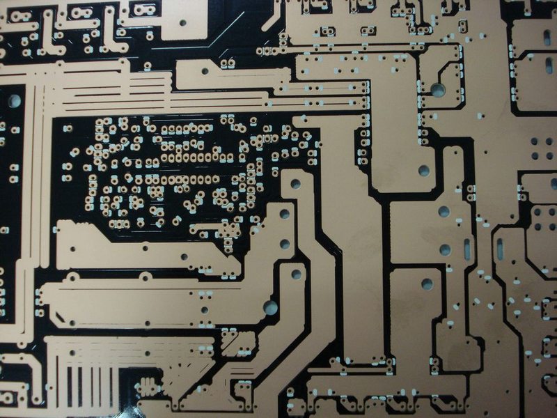
Immersion Tin is the lead-free alternative to the Hot Air Leveling(Hasl) process on pcbs. On printed circuit board surface and the
bore holes,the thickness of Tin is between 0.7 μm and 1um.
The tin layer protects untreated copper from oxidation; it is a perfect foundation for soldering applications, as well as for plug
contacts during the production of Printed circuit Board.
Within the electronics industry,immersion tin is recognized as a reliable surface finish for both PCBs and IC substrate applications.
It is used in many market segments, such as automotive, communications, consumers and industrial electronics.
Mutilayer printed circuit board
FR4 1.60mm Material
1OZ finish Copper
Immersion Tin surface finish
Min Track/Space: 8mil
Min Hole: 0.4mm
Routing outline
2 Layer pcbs
FR4 2.40mm thickness
1OZ base copper
Immesion Tin surface finish
Min line/width: 10/12mil
Min Hole Size: 0.20mm
Black soder mask


 Immersion Tin PCB