Double sided pcbs, common in both production and prototype circuits, allow a higher density in components and make layering of
tracks an easier process.
Compared to multilayer pcbs, double layer pcbs do not need lamination, but need plating in order to reach through hole function.
Double sided printed circuit boards are made with a substrate of non-conductive material, over which a layer of copper is placed
on top and the bottom of it, and in the case of double sided boards, the copper is also layered on the bottom side of the substrate.
The circuits on top and bottom layers are connected by a "bridges" called the guide hole (via), which is also called plated through
hole (PTH), and the hole without connecting function is called NPTH holes because there is no metal in hole.
Please visit Conventional PCB to check our Doulbe Sided PCB capability list
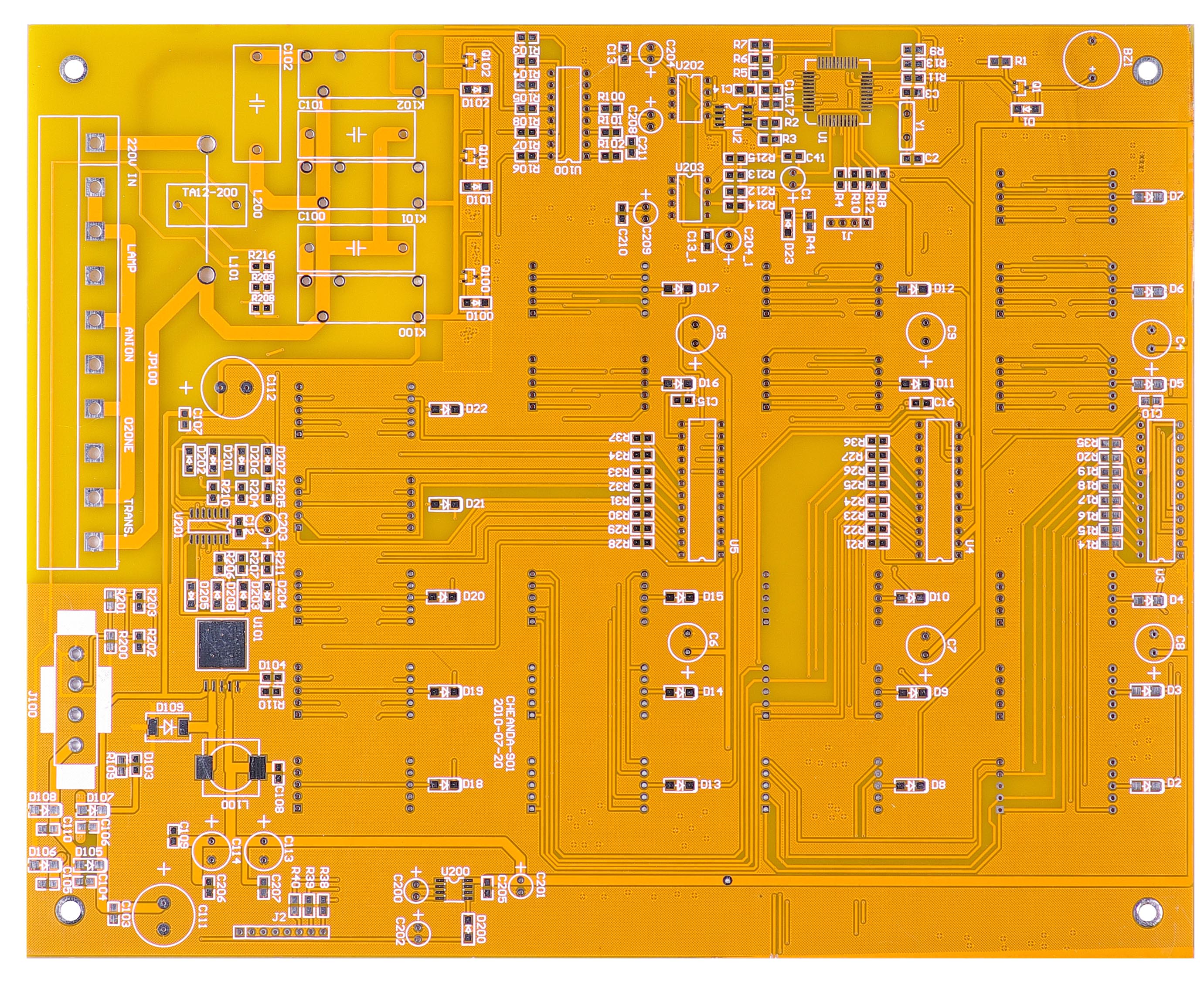
2 Layer pcbs
FR4 1.55mm board thickness
2oz finish copper
Lead Free Hasl surface finish
Min Track/Space: 8mil
Min hole size: 0.18mm
Green Solder Mask
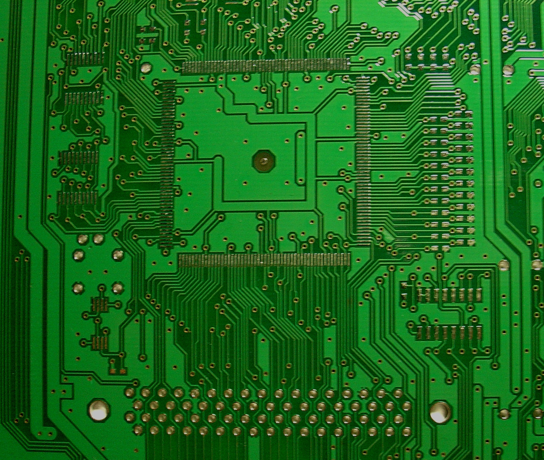
Double Sided Printed Circuit Board
FR4 1.60mm Board Thickness
1OZ base copper thickness
L/F HAL Finish surface treatment
Min Line/Width: 6mil
Min Hole Size: 0.25mm
Yellow Solder Mask


 Double Sided PCB