Blind holes start on an outer layer but terminate on an inner layer. Buried Vias exist only between inner layers but do not begin or
terminate on an outer layer. Blind & Buried vias can be divided into two kinds, mechanical and laser.
Blind and buried vias help to reach PCB density by allowing features and lines to be designed above or below them without making
a connection. Lots of fine pitch BGA and flip-chip component footprints do not allow for running traces and through. Instead, the blind
and buried vias will only connect those layers that are required to have a connection in that specific area, allowing for PCB real estate
space savings.
Blind and buried vias PCB, also known as HDI boards, often used for mobile phones, GPS navigation, wireless product, MID. Notebook.
etc.
Please click HDI PCB to check our blind & buried hole capability list.
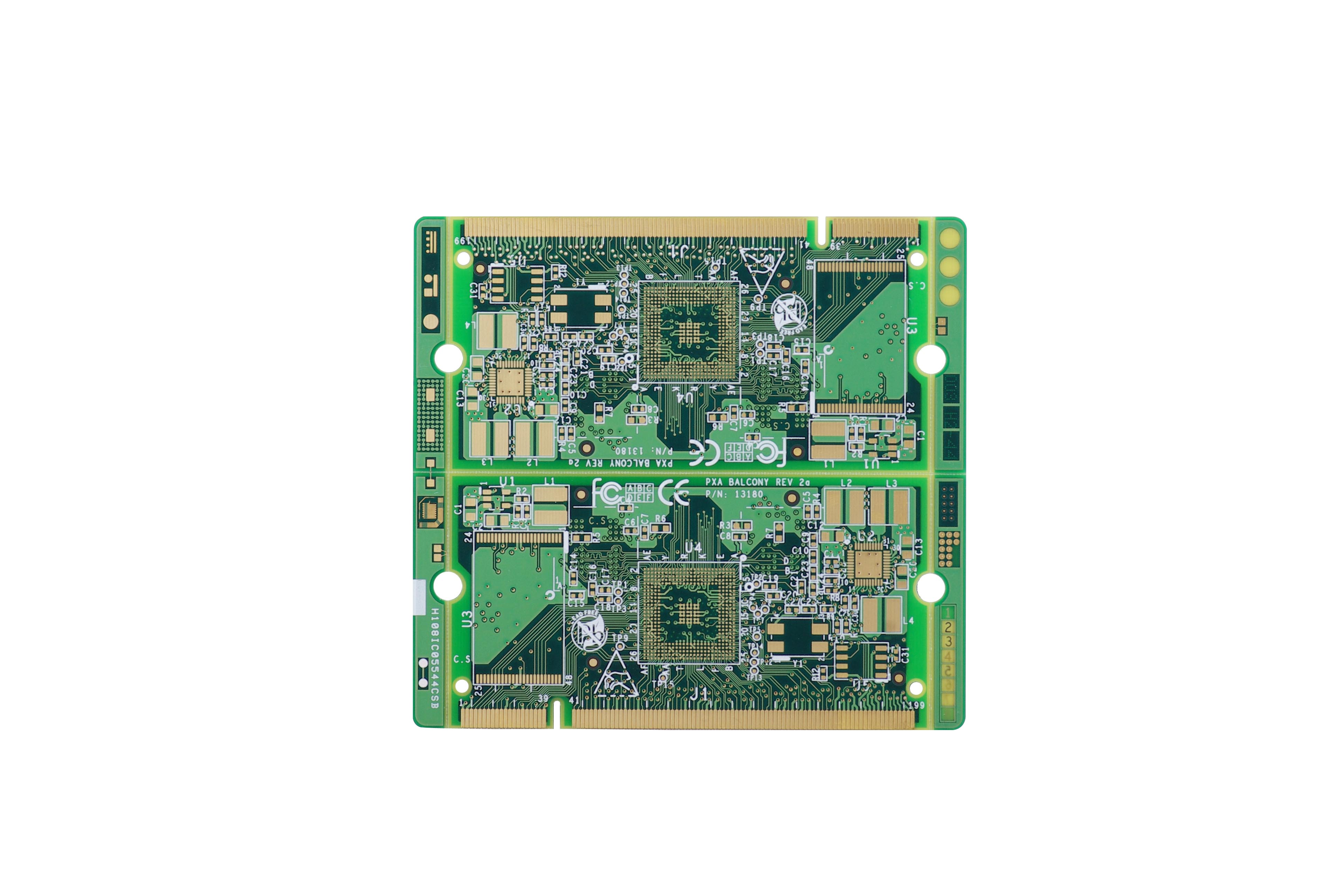
8 Layer Blind Holes Printed Circuit Board
1+6+1 Stack up
FR4 1.0MM Thickness
1OZ finish Copper thickness
Immersion Gold Finish
Min Line/Space 3/3 mil
Gold Finger
Designed for Note Book
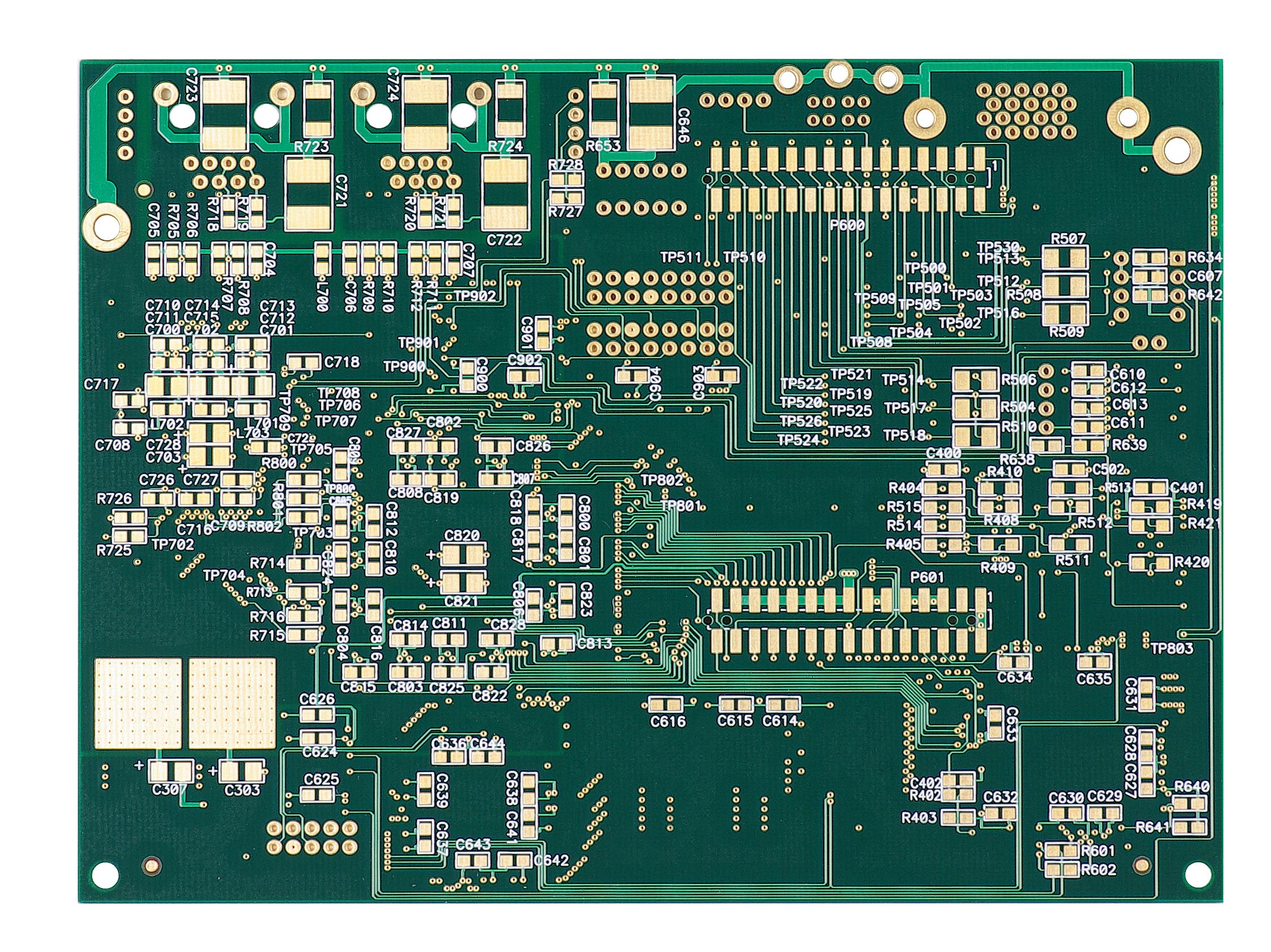
4 Layer Blind pcb
1+2+1 Stack up
FR4 1.6MM Thickness
3OZ finish Copper thickness
Immersion Gold Finish Surface Treatment
Min Line/Space 8/8 mil


 Blind & Buried PCB