The quick development of electronics has high requirement to printed circuit board, which single sided or double sided
printed circuit board cannot reach, thus, multilayer pcbs were designed. Printed circuit board with four or more circuit line
is called multilayer pcbs or multi-layer printed circuit board.
Production of multilayer inner graphics in place first, and then made single-sided or double-sided substrate etching printed
and included in the specified layer, and then by heat, pressure and be bonded, as to the subsequent drilling Kong is the
same and double-sided plated through hole method. These basic methods of production and construction method dating
back to the 1960s, not much changed, but with the materials and process technologies (for example: lamination bonding
technique to solve drilling, glue residue, the improvement of the film) become more mature, the accompanying even more
diversification to the characteristics of the multilayer.
Mutilayer pcb are widely used in high technology project such as computer,industrial control, telecommunication, power
supply,digital products, medical, automobile, aerospace and so on.
Please visit Conventional PCB to check our capability list for mutilayer pcbs
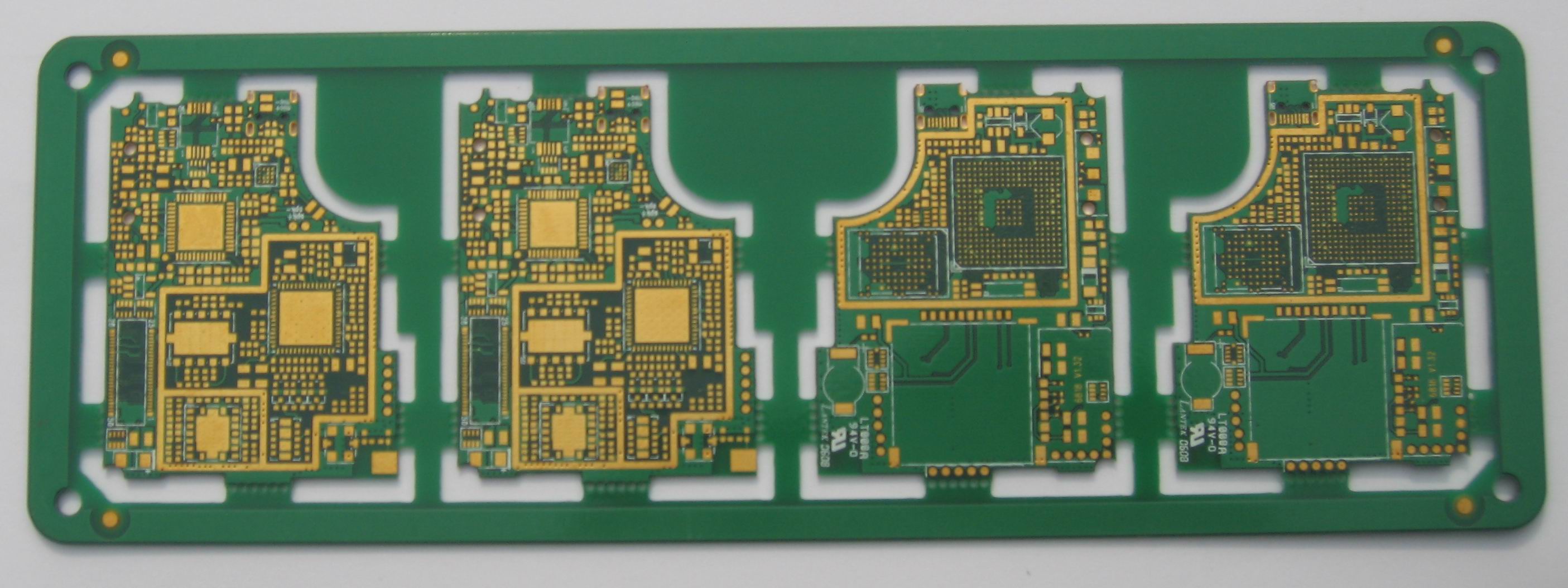
Multilayer pcbs (4 layer)
FR4 1.60mm board thickness
1OZ finish copper
Immerson Gold finish
Min track/space: 8mil
Min hole size: 0.23mm
Green Solder Mask
Outline: Routing
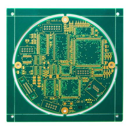
Mutilayer Printed Circuit Board (6 Layer)
FR4 2.00mm board thickness
1OZ base copper thickness
Immersion Gold surface treatment
Min line/width: 10mil
Min Hole size: 0.27mm
BGA
Complicated Routing Outline.


 Multilayer PCB