Home | Favorites | 中文 | Deutsch |
|
  |
|
   |


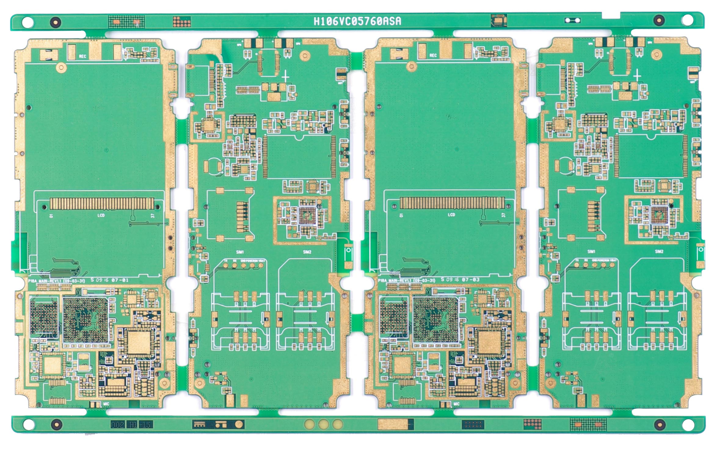
 Mobile Phone PCB Mobile Phone PCB |
 |
|
|
|
The continuous trend towards further miniaturization in electronics inevitably leads to a growing integration density and
cell phone is the one that shows this in morden life. In order to reach more function on a smaller electronics, HDI pcs were
designed and produced.
As an authorized agent of Foxconn , we are specializing in providing HDI PCB for many years.
The following leading technologies make us the top supplier for customer’s HDI demand.
HDI PCB fabrication
Via in pad
Any layer interconnection
Blind and Buried via
plus III laser drilling
Copper filling to blind via
2.5mil fine line and space
Skipped and stepped holes
Please visit HDI PCB to check our capability list for cell phone pcbs.
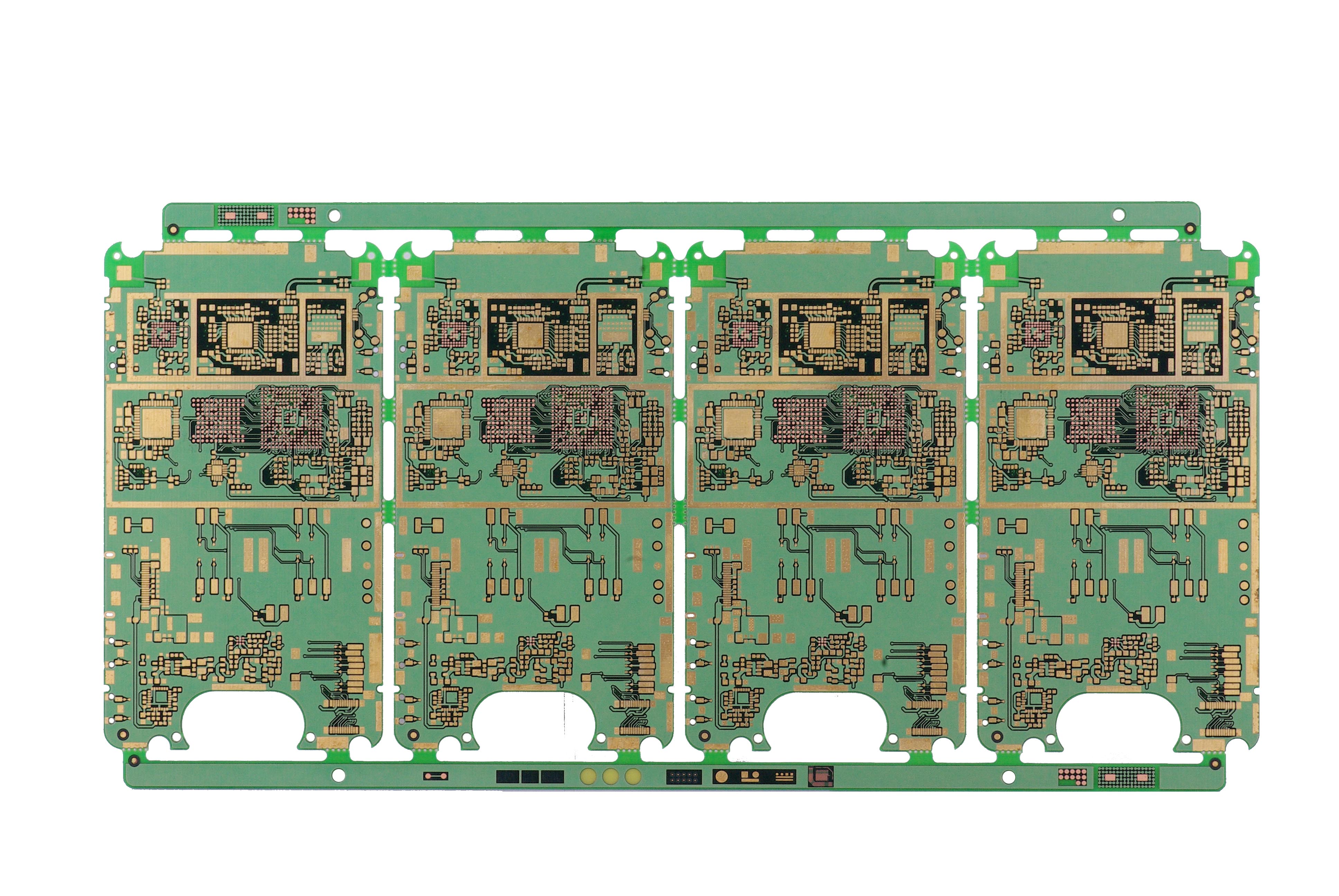
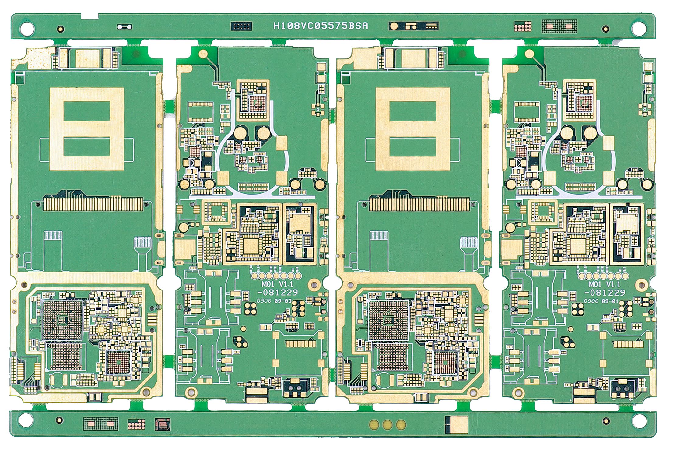
8 Layer Printed Circuit Board 6 Layer pcbs
FR4 1.0MM Board Thickness FR4 1.0MM Board Thickness
Immersion Gold + Selective OSP Immersion Gold + Selective OSP
Stack up 2+4+2 Stack up 2+2+2
Min Track/Width 3/3mil Min Track/Width 3/4mil
Buried Holes Buried Laser Holes
Designed for Cell Phone Designed for Cell Phone
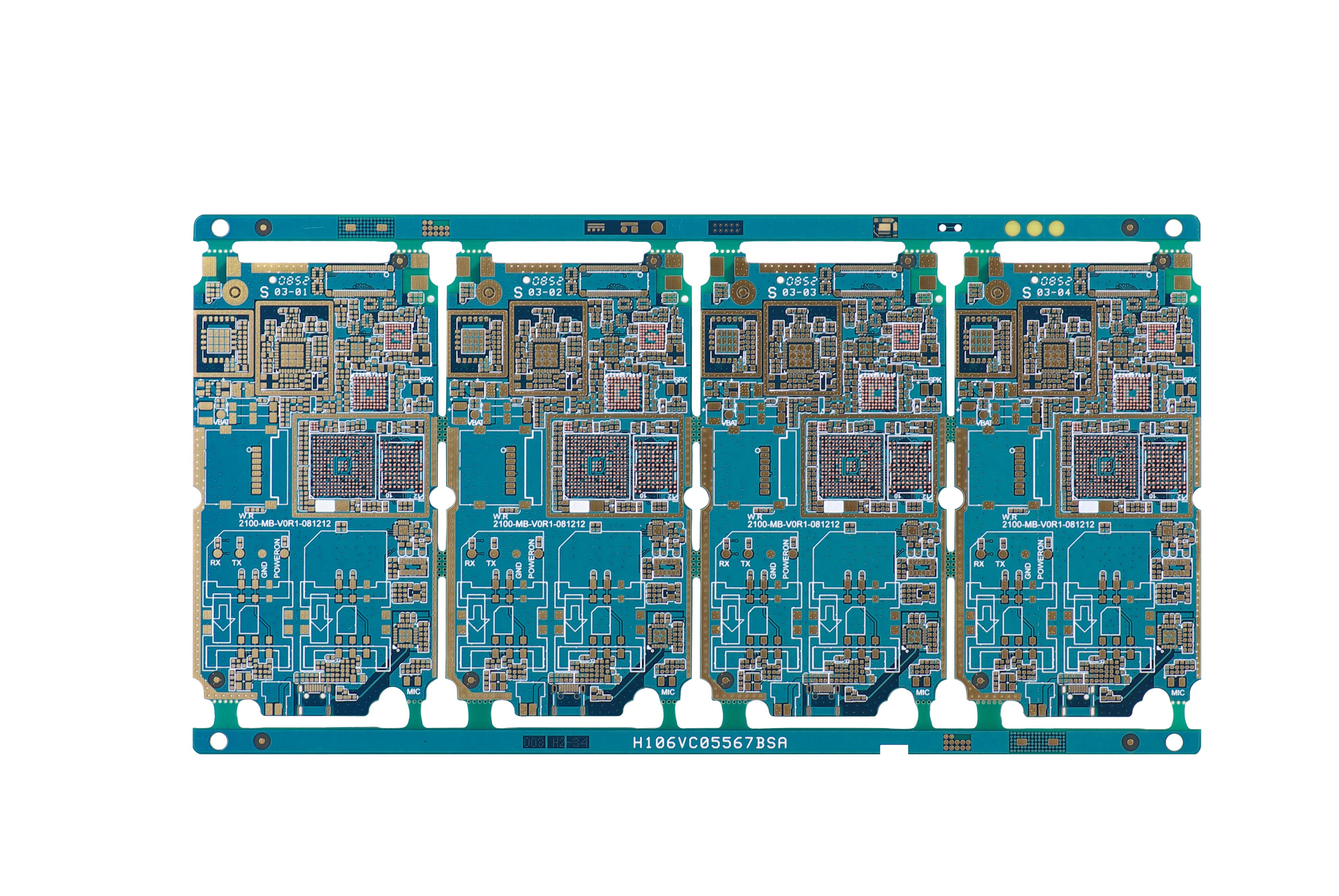
4 Layer pcb 10 Layer pcbs
FR4 1.0MM Board Thickness FR4 1.0MM Board Thickness
Immersion Gold + Selective OSP Immersion Gold + Selective OSP
Stack up 1+2+1 Stack up 2+6+2
Min Track/Width 3/2.5mil Min Track/Width 3/4mil
Buried Holes Blind Laser Holes
Used for Cell Phone Designed for Mobile Phone
