Impedance is the sum of the resistance and reactance of an electrical circuit expressed in Ohms, the most common example
of a controlled impedance component is the downlead (or feeder) connecting a receiving aerial to a wireless or television set.
As the speed of signal switching on a PCB increases, the electrical properties of the traces carrying signals between devices
become increasingly more important.
For bare board pcbs, we can do single ended impedance control and differential impedance control pcbs, and the best tolerance
we can do now is ±5%.
The characteristic of Impedance control PCB
According to the theory of signal transmission, the signal is a function of time, distance variables, so the signal may change every part
of the connection. Therefore, to determine the connection of the AC impedance, ie, voltage changes and current changes in the ratio of
the transmission line characteristic impedance transmission line characteristic impedance (Characteristic Impedance): connection
with the signal itself features. In the actual circuit , wire resistance value is less than the impedance of the system of distribution , Utah
Resistive Plate The high-frequency circuits , the characteristic impedance depends on the connection unit of the distributed capacitance
and impedance of the distribution of unit distributed inductance . The ideal transmission line characteristic impedance depends only on
the connection of units distributed capacitance and units distributed inductance
Please visit
HDI PCB to check our impedance control capability.
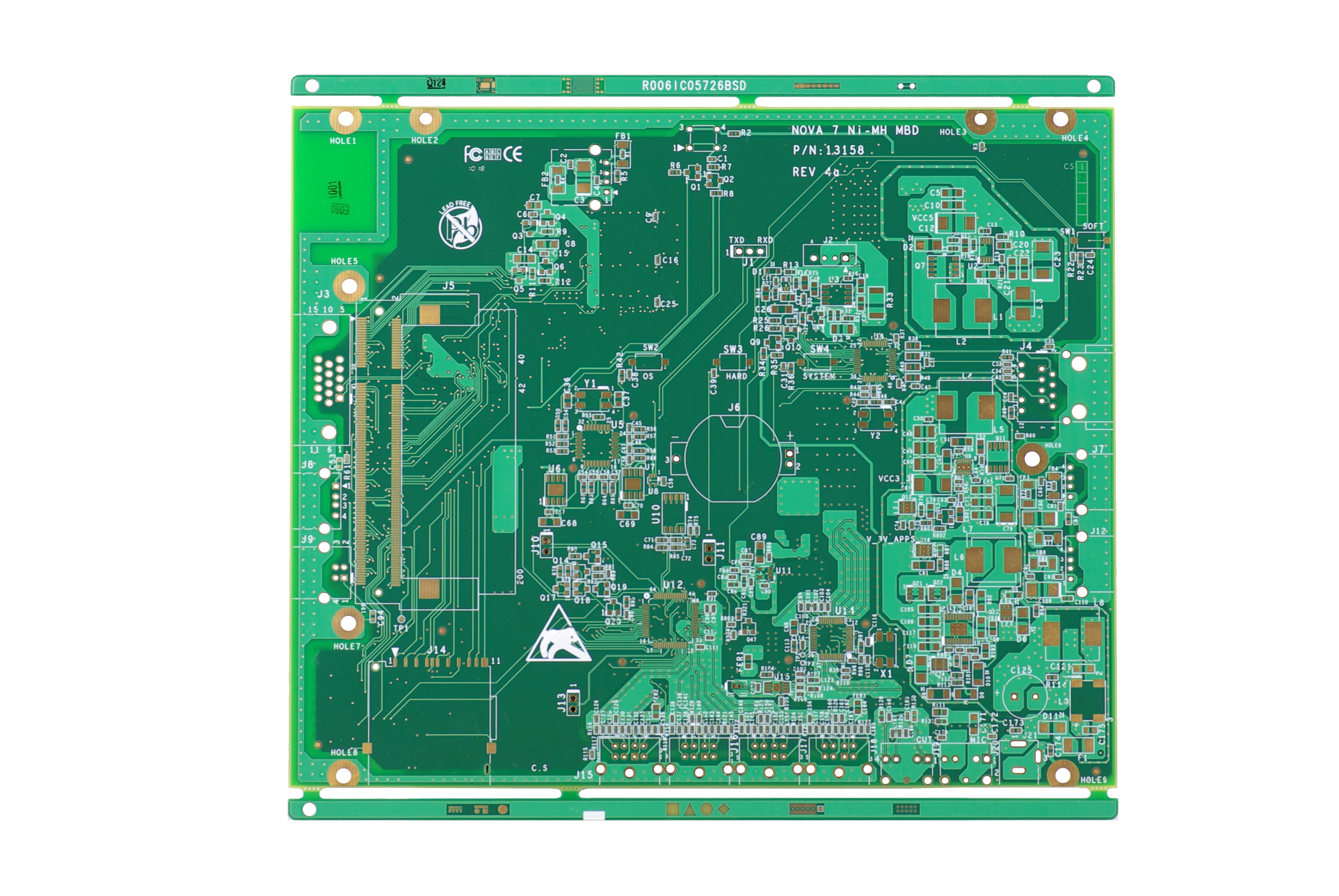
6 Layer Impedance Control pcb
FR4 1.60MM 1oz finish copper
Immersion Gold Surface Finish
90 ,55, & 60 ohm Single Ended
90 Ohm Differential
Min Track/Width: 3/3Mil
BGA Pad & Via on the Pad
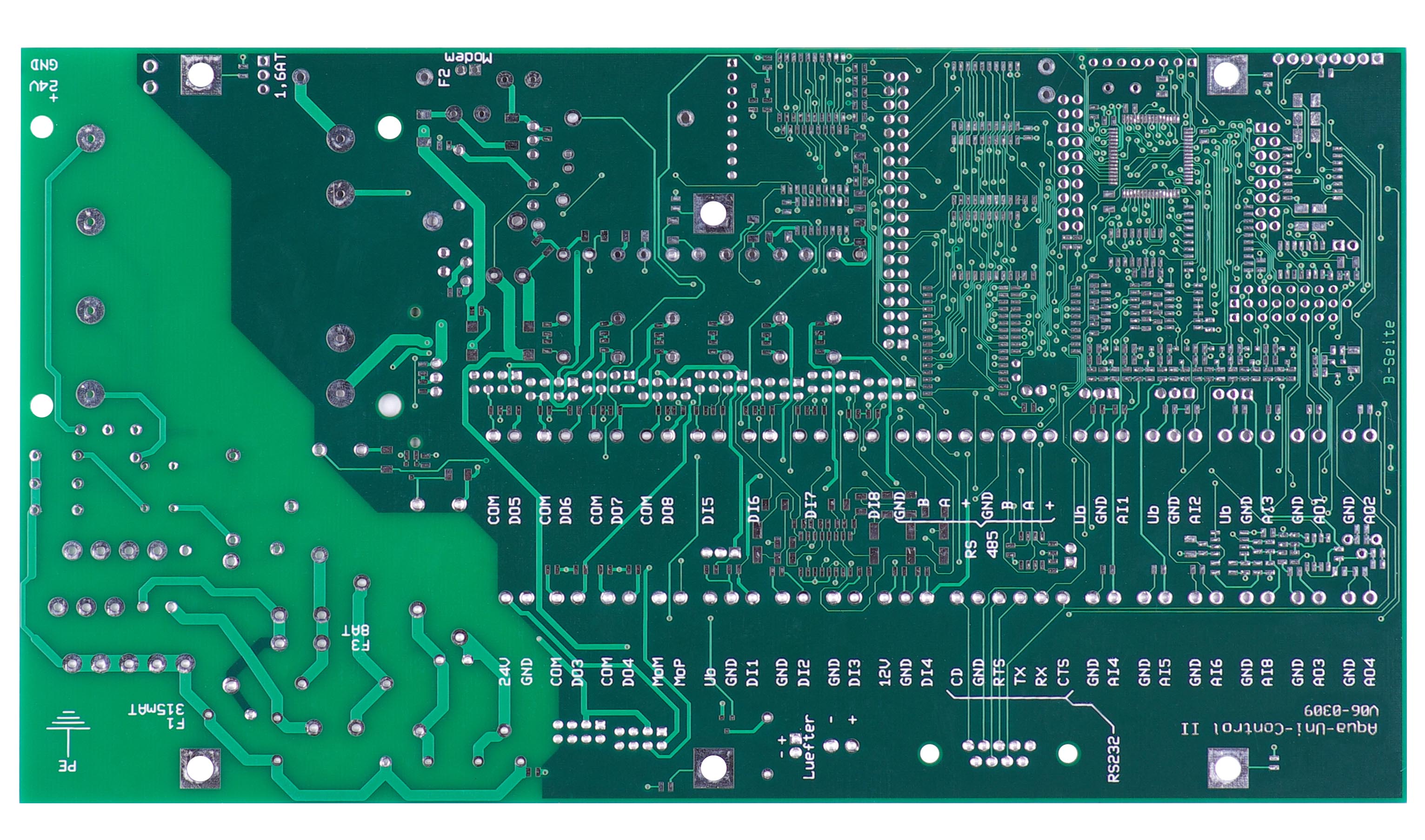
8 Layer Printed Circuit Board
FR4 1.60mm Board thickness
1.5 OZ finish copper thickness
Lead Free Hasl Finish
75 Ohm Single ended Impedance Control Value
Min Hole: 0.30mm
Min Track/Space: 5/5 mil
Green Solder Mask


 Impedance Control PCB